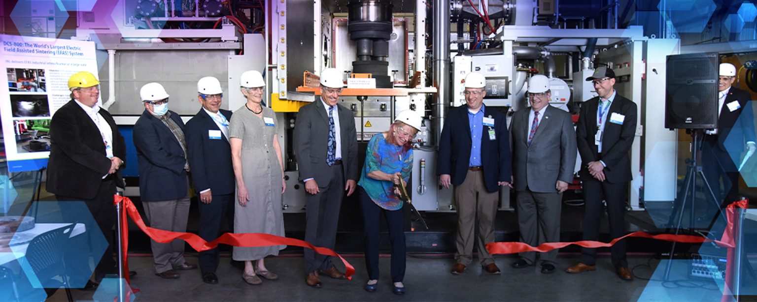
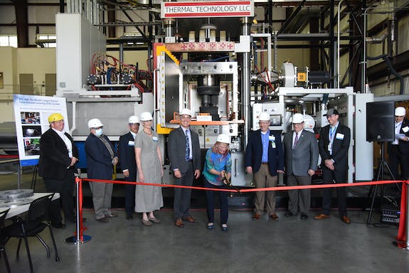
The future of the manufacturing industry depends on advancements that lead to decarbonization. At Idaho National Laboratory, a ribbon cutting event recently unveiled first-of-its-kind electric field assisted sintering (EFAS) technology. At the event, the lab showcased the world’s largest direct current sintering equipment, DCS-800.
The availability of the DCS-800 will allow for more cost-effective, time-efficient manufacturing of metals and ceramics, using a process that produces lower carbon emissions. The manufactured materials are designed to withstand extreme conditions at industrial-length scales. Such materials must meet exacting specifications for use in technology such as wind turbines, spacecraft, nuclear energy, protective systems and hydrogen cells.
EFAS technology is similar to traditional hot-pressing methods for developing these materials. However, hot-pressing is less efficient and consumes more energy to achieve the same results. The differences in hot-pressing contribute to longer heating periods and higher costs that limit the widespread use of advanced materials in everyday items such as automobiles. Spark plasma sintering, the technology used in the DCS-800, offers greater material integrity while also reducing energy consumption, carbon emissions and subsequent costs.
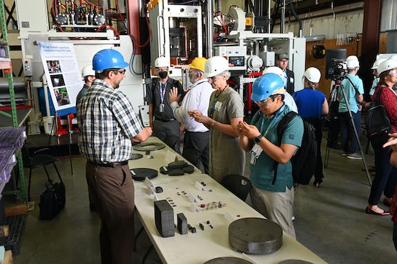
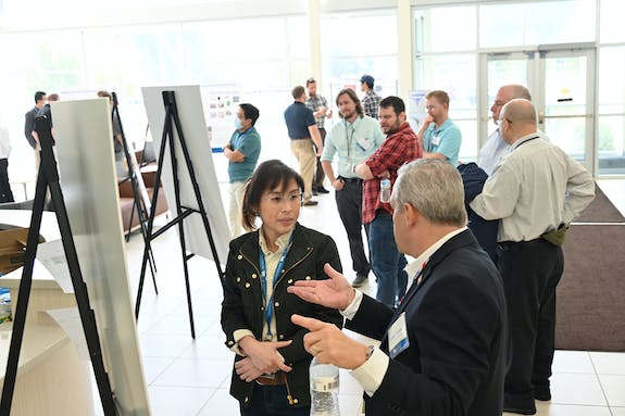
The ribbon-cutting event showcased the technology with listening sessions and poster presentations focused on detailing its capabilities and related research being performed at INL. Representatives from industry, academia, the U.S. departments of Energy and Defense attended. Community leaders including INL Director John Wagner and Ammon Mayor Sean Coletti delivered remarks.
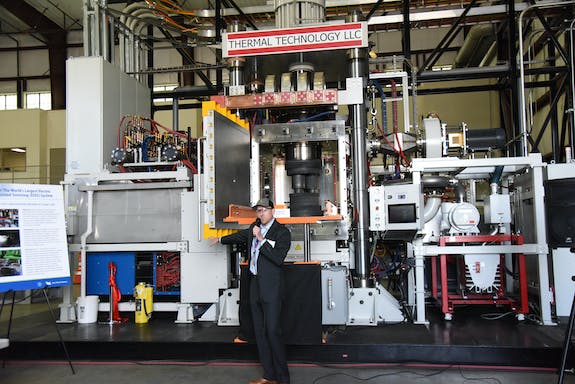
“Because of its size and capabilities — operating at high power, high temperatures and high pressure — the DCS-800 will enable many of today’s high-performance technologies that require advanced materials,” said Wagner. “New capabilities to design and manufacture materials strategically and rapidly with predicted performance in extreme environments have the potential to accelerate advancements in nuclear energy, aerospace and defense areas.”
EFAS sends electricity through the sample die — sometimes through the material itself if electrically conductive — to heat up and fuse individual particles of powdered metals, ceramics or a mixture of both, making incredibly durable materials.
Anthony Nickens, Materials and Manufacturing Science and Technology director said, “The new DCS-800 capability is faster and more cost-effective than traditional powder metallurgy and diffusion bonding methods. Now that this technology is available for our partners to use, we expect to see a lot of growth and collaboration developing the technique for the materials manufacturing space.”
By harnessing the power of the DCS-800 at INL, U.S. companies can remain competitive in advanced manufacturing, innovating processes that consume less energy while maintaining or improving quality.
Located at INL’s Energy Systems Laboratory, the DCS-800 can make parts up to 2 feet in diameter. It allows materials that have been tested at bench scale to be demonstrated at industrially relevant scales.
“INL has a demonstrated track record of conducting great science that helps industry move products into the marketplace, where they can improve lives,” said Wagner.
For more information, check out the electric field assisted sintering fact sheet on INL.gov.

